Half Adder and Full adder

A digital computer performs different operations with devices like half adder, full adder, half subtractor, full subtractor, parallel adder, BCD adder, multiplexer, demultiplexer, decoder, encoder, code converters, etc. Theses circuits are called as combinational circuits.
In this post, you will learn about Half adder and Full adder circuit in detail. Before, going into this topic, let us learn something about combinational circuit?
What is a combinational Circuit?
A combinational circuit is a digital circuit which produce an output depending on the specified combination of input variables, with no storage devices involved. The output of these circuits at any time, depend only on the present state of input variables.
Generally, a combinational circuit consist of inputs, logic gates and outputs. The logic gates accept the input and produces the required output.

The combinational circuit accepts n-input binary variables and generates m-output variables depending on the combination of logic gates.
Design of a combinational circuit
The design of the combinational circuits involves commence by defining the problem of the circuit and ends in the formation of boolean function or constructing a truth table or a logical circuit diagram.
Follow the below procedure to design procedure of the combinational circuit.
- Defining the problem of a circuit
- Determine the number of available inputs and required output variables.
- Assign letter symbols to input and output variables.
- Derive the truth table indicating the relationship between input and output variables.
- Obtain simplified Boolean expression for each output.
- Implement it, with a logic diagram.
Half Adder
Before proceeding to the topic, you have to know about Binary addition. Learn how to add two binary numbers.
The half adder circuit needs two binary inputs(Augend bit and addend bit), two binary outputs(sum and carry) and combination of logic circuit to produce the output.

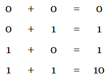
It performs addition operation of two bits. Four possible operations are possible with the two inputs and produces four outputs, as shown below.

As you can see, single bit output is produced for the first three operations, but two bits are produced for the last operation. The most significant bit(MSB) of the two digit output is called carry and least significant bit(LSB) is called Sum.
The truth table for half adder is shown below.

For sum and carry outputs, a boolean expression has to be derived using Karnaugh map. Since it has only two input variables, 4-cells k-map is used to simplify. Learn how to Minimize a Boolean function using k-map.

The obtained boolean expression for sum output is nothing but an Ex-OR gate. The Logic circuit diagram for the obtained boolean expression is shown below.

Demerit of Half adder
Adding of two bits using half adder does not cause any problem. But when adding two bits along with the carry from the addition operation of previous digits, half adder is not suitable.

Half adder cannot be able to do such computations. Full adders overcome the demerit of half adder.
Full adder
The full adder circuit needs three binary inputs(two binary inputs and one carry bit from the previous addition), two binary outputs(sum and carry) and combination of logic circuit to produce the output.

It performs addition operation of three bits. Eight possible operations are possible with three inputs and produces eight, 2 digit outputs. The MSB of the two digit represents carry and LSB represents sum. The truth table for full adder is shown below.

For sum and carry outputs, boolean expression has to be derived using Karnaugh map. Since it has only three input variables, 8-cells k-map is used to simplify.

The obtained boolean expression for sum output can still be simplified as below.

Now we have two boolean expressions for sum and carry output. With those expressions, the combinational circuit for full adder is constructed.

Realization of full adder with two half adders
The full adder can be implemented with two half adders by cascading them. The sum output of first half adder is Ex-OR of A and B. The sum output of full adder is Ex-OR of Cin and output of first half adder.
The carry output of the full adder can be realized as below from the obtained boolean expression. Refer Postulates and Theorems of Boolean Algebra for the below simplification.

The full adder can be realized as below. The truth table for the below full adder circuit is the same as the one discussed above.


I think the schematics “Logic circuit for Full adder” ia wrong. An XOR with three inputs throws a sum of 0, when all inputs are 1.
No, it is correct. When all the three inputs are 1,
Ex-or of two input, A ⊕ B = 1 ⊕ 1 = 0
Now, Cin ⊕(A ⊕ B) = 1 ⊕ 0 = 1