Phasor diagram of practical transformer on Load

A practical or actual transformer will have winding resistance and leakage reactances both on the primary and secondary sides. When the secondary of the transformer is connected to the load terminals, the transformer is said to be on load. The load can be either resistive, inductive, or capacitive. In this section, let us learn the phasor diagram of practical transformer on load condition.
Let us consider a practical transformer as shown below, which has primary and secondary windings of resistances R1 and R2 and reactances X1 and X2 respectively.

In the above circuit, V1 and I1 are the primary voltage and current respectively, E1 is the induced emf in the primary winding and N1 is the number of turns in the primary winding. Similarly, N2 is the number of turns in the secondary winding, E2 is the induced emf in the secondary winding, V2 is the terminal voltage and I2 is the load current in the secondary winding.
The impedance of primary winding and secondary winding is given by,
![]()
![]()
Before drawing the phasor diagram of the transformer on load, it is important to learn the operation of transformer on load condition.
Steps to draw the phasor diagram
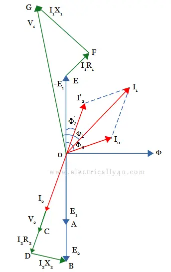
The below diagram shows the phasor diagram of the transformer on resistive load. Follow the below procedure to draw the diagram.
- Consider the flux Φ as the reference phasor.
- The EMF induced in the transformer E1 is drawn lagging the flux(Φ) by 900 as OA.
- The counter-induced emf(-E1) in the primary winding is drawn equal and opposite to E1.
- Due to winding resistance and leakage reactance, the secondary current I2 lags behind the induced emf E2 and is drawn as OI2.
- Since the load is resistive, secondary voltage V2 is drawn in phase with I2 as OC.
- The voltage drops due to winding resistance(I2R2) in the secondary is drawn parallel to the secondary current phasor I2 from V2 phasor as CD = I2R2.
- Similarly, the voltage drop due to reactance(I2X2) in the secondary winding is drawn perpendicular to the current phasor I2 from D as DB = I2X2.
- Now, the phasor sum of terminal voltage V2, voltage drop due to secondary resistance I2R2, and voltage drop due to secondary reactance I2X2 is equal to induced emf E2 in the secondary winding. Its magnitude is expressed as,
![Rendered by QuickLaTeX.com \[E_2 = V_2 + I_2(R_2 + j X_2) = V_2 + I_2 Z_2 \]](data:image/svg+xml;base64,PHN2ZyB4bWxucz0iaHR0cDovL3d3dy53My5vcmcvMjAwMC9zdmciIHdpZHRoPSIyODUiIGhlaWdodD0iMTkiIHZpZXdCb3g9IjAgMCAyODUgMTkiPjxyZWN0IHdpZHRoPSIxMDAlIiBoZWlnaHQ9IjEwMCUiIHN0eWxlPSJmaWxsOiNjZmQ0ZGI7ZmlsbC1vcGFjaXR5OiAwLjE7Ii8+PC9zdmc+)
- The current in the primary winding has two components: no-load current(I0) and load component of the primary current(I2‘).
- Draw the no-load current I0 by lagging -E1 by no-load angle Φ0.
- Since I2‘ is the load component of the primary current, it is drawn equal and opposite to I2.
- The phasor sum of I0 and I2‘ gives the primary current I1.
- The voltage drops due to winding resistance(I1R1) in the primary is drawn parallel to the primary current phasor I1 from -E1 phasor as EF = I1R1.
- Similarly, the voltage drop due to reactance(I1X1) in the primary winding is drawn perpendicular to the current phasor I1 from D as FG = I1X1.
- Now, the phasor sum of counter-induced emf -E1, voltage drop due to primary resistance I1R1, and voltage drop due to primary reactance I1X1 gives the applied voltage V1 to the primary winding. Its magnitude is expressed as,
![Rendered by QuickLaTeX.com \[V_1 = -E_1 + I_1(R_1 + j X_1) = -E_1 + I_1 Z_1 \]](data:image/svg+xml;base64,PHN2ZyB4bWxucz0iaHR0cDovL3d3dy53My5vcmcvMjAwMC9zdmciIHdpZHRoPSIzMTQiIGhlaWdodD0iMTkiIHZpZXdCb3g9IjAgMCAzMTQgMTkiPjxyZWN0IHdpZHRoPSIxMDAlIiBoZWlnaHQ9IjEwMCUiIHN0eWxlPSJmaWxsOiNjZmQ0ZGI7ZmlsbC1vcGFjaXR5OiAwLjE7Ii8+PC9zdmc+)
- The phase angle Φ1 between V1 and I1 gives the power factor angle of the transformer.

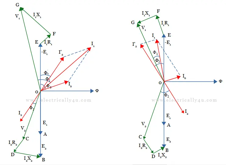
The same procedure is repeated for inductive load and capacitive load. However, in the case of inductive load, secondary voltage V2 is drawn leading the secondary current I2 by an angle Φ2 as OC. In the case of capacitive load, secondary voltage V2 is drawn lagging the secondary current I2 by an angle Φ2 as OC.

From the phasor diagrams, the following equations can be derived.
(a) For pure resistive load,
![]()
![]()
![]()
Using the transformation ratio,
![]()
(b) For resistive-inductive load,
![]()
![]()
![]()
![]()
(b) For resistive-capacitive load,
![]()
![]()
![]()
![]()


